
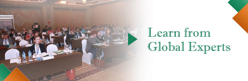
Webinar on
Nanomaterials and Technology
September 19, 2020
Nanomaterials 2020
Theme: New Advanced techniques in the field of Nanomaterials
We are delighted to invite all the participants globally to attend “Webinar on Nanomaterials which is going to be held by Meetings International during 24 September, 2020 which includes incite keynote and oral Presentation. It emphasizes on the theme "Techniques for learning the new technologies in the field of Nanophononics". It provides a premier technical forum for reporting and learning about the latest research and development, as well as for launching new applications and technologies. The principle focal point of nanomaterials is the thriving to vary the analysis cycle in optics, nanophotonic and lasers.
Session 1: Nanophotonics & Plasmonic
Nanophotonics & plasmonics focuses on light at the nanometer-scale. Light can only be focused to a spot roughly half its wavelength in size (a few hundred nanometers for visible light). This limit can be surpassed by coupling light to electrons at the surface of a metal and creating surface plasmons. This area of nanoscience, called nanophotonic, is defined as “the science and engineering of light matter interactions that take place on wavelength and sub wavelength scales where the physical, chemical or structural nature of natural or artificial nanostructured matter controls the interactions”.
Session 2: Nanofabrication and characterization
Nanofabrication is the design and manufacture of devices with dimensions measured in nanometers. One nanometer is 10 -9 meters, or a millionth of a millimeter. Nanofabrication is of interest to computer engineers because it opens the door to super-high-density microprocessor s and memory chips. It has been suggested that each data bit could be stored in a single atom. Carrying this further, a single atom might even be able to represent a byte or word of data. Nanofabrication has also caught the attention of the medical industry, the military, and the aerospace industry. The market for nanofabrication equipment will grow at a compound annual growth rate of 10.4 percent over the period 2009 to 2014 and reach $90.4 billion in that year, according to Innovative Research and Products Inc. (Stamford, Connecticut).Over the same period the market for semiconductor wafers will grow at a CAGR of 14 percent to double and reach $20.6 billion in that year, the company said.
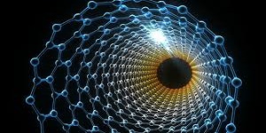
Session 3: Advance Nanomaterials
Nanomaterials are defined as materials with at least one external dimension in the size range from approximately 1-100 nanometers. Nanoparticles are objects with all three external dimensions at the nanoscale1. Nanoparticles that are naturally occurring (e.g., volcanic ash, soot from forest fires) or are the incidental byproducts of combustion processes (e.g., welding, diesel engines) are usually physically and chemically heterogeneous and often termed ultrafine particles. Engineered nanoparticles are intentionally produced and designed with very specific properties related to shape, size, surface properties and chemistry. These properties are reflected in aerosols, colloids, or powders. Often, the behavior of nanomaterials may depend more on surface area than particle composition itself. World demand for nanomaterials will rise more than two-and-a-half times to $5.5 billion in 2016. Nanotubes, nano clays and quantum dots will be the fastest growing types. The energy storage and generation and construction markets will offer the best growth prospects. China, India and the US will lead gains among countries. This study analyzes the $2 billion world nanomaterial industry. It presents historical demand data for the years 2001, 2006 and 2011, and forecasts for 2016 and 2021 by material (e.g., metal oxides, chemicals and polymers, metals, nanotubes), market (e.g., health care, electronics, energy generation and storage, construction), world region and for 15 countries.
Session 4: Nanoelectronics and Microsystems
Nanoelectronics holds some answers for how we might increase the capabilities of electronics devices while we reduce their weight and power consumption. Improving display screens on electronics devices. This involves reducing power consumption while decreasing the weight and thickness of the screens. Increasing the density of memory chips. Researchers are developing a type of memory chip with a projected density of one terabyte of memory per square inch or greater. Reducing the size of transistors used in integrated circuits. One researcher believes it may be possible to "put the power of all of today's present computers in the palm of your hand”. Microelectronics is one of the main subfields of electronics. As the name indicates, microelectronics is highly related to the study and manufacture of microfabrication of very small electronic components. Micro-sensors that combine optical and mechanical sensor functions with integrated electronic signal processing are rapidly growing in areas such as safety, health, environmental monitoring, and energy control. Relevant examples are collision sensors for airbags and instruments for endoscopy. The global market for nanoelectronics is expected to reach $409.6 billion by 2015, as stated by the new market research report. Nanoelectronics is expected to exercise a considerable influence on semiconductors, displays, memory and storage devices and communication devices.
Session 5: Nanomedicine and Nanobiotechnology
Molecular nanotechnology has been defined as the three-dimensional positional control of molecular structure to create materials and devices to molecular precision. The human body is comprised of molecules; hence the availability of molecular nanotechnology will permit dramatic progress in human medical services. More than just an extension of "molecular medicine," Nanomedicine will employ molecular machine systems to address medical problems, and will use molecular knowledge to maintain and improve human health at the molecular scale. Nanomedicine will have extraordinary and far-reaching implications for the medical profession, for the definition of disease, for the diagnosis and treatment of medical conditions including aging, and ultimately for the improvement and extension of natural human biological structure and function. “Nanomedicine is the preservation and improvement of human health using molecular tools and molecular knowledge of the human body. “Nanobiotechnology is a new frontier for biology with important applications in medicine. It bridges areas in physics, chemistry, and biology and is a testament to the new areas of interdisciplinary science that are becoming dominant in the twenty-first century. This course provides perspective for students and researchers who are interested in nanoscale physical and biological systems and their applications in medicine. It introduces concepts in nanomaterials and their use with biocomponents to synthesize and address larger systems. Applications include systems for visualization, labeling, drug delivery, and cancer research.
Session 6: Nanotechnology in energy and environment
Research into hydride materials for energy applications typically focuses on enhancing gravimetric storage density and ion transport of the materials. However, the requirements for stationary applications such as fuel cells can be significantly different and amenable to a broader class of potential materials. Multiple geophysical and social pressures are forcing a shift from fossil fuels to renewable and sustainable energy sources. To effect this change, we must create the materials that will support emergent energy technologies. Solar energy is the utmost priority to develop photovoltaic cells that are efficient and cost effective. Department of Materials Science and Engineering, Stanford University, conducting extensive research on Photovoltaics, Energy storage and Hydrogen storage to meet global Energy requirements.
- Nano spectroscopy
- Nanofabrication and characterization
- Advance Nanomaterials
- Nanoelectronics and Microsystems
- Nanomedicine and Nanobiotechnology
- Nanotechnology in energy and environment
- Applications of Nanotechnology
- Industrial Nanotechnology
- Nano-Micro Electronics, Metamaterials & Quantum Technology
- System Engineering, Computer Technologies, Telecommunications Engineering & Signal Technology
- Nano spectroscopy
- Journal of Materials Science and Nanomaterials
- Journal of Nanomaterials & Molecular Nanotechnology
- Journal of Nanoscience & Nanotechnology Research

fgsg
tgh

Dear Eliza, Thank you for that wonderful opportunity given to share my experiences during the conference. I would like to place on record the smooth conduct of the conference. My appreciation goes a long way to Eliza for her timely communication and well advanced information disseminated processes. The presentation schedule and the time mentioned in the mail sent were also strictly followed. All the best. Regards Kalyani Kenneth Speaker | Psychiatry-2021
Kalyani Kenneth

Dear Laura, Thank you for giving me the opportunity to present my current work! I really enjoyed listening and connecting to a wider international scientist through this conference. And I am really looking forward for the physical conference next year! Best regards Sharmaine
Sharmaine Reintar

Many thanks Laura. It iş my plesure work with you
Pinar Kara

It was my pleasure to be a part of the conference. The talks were technically profound. Thank you once again.
Anupam Mukherjee

Thank you very much for the message. I am glad that the presented poster was appreciated. I'm also grateful for the certificate. Dispite my main work was the subject presented in the session, it would be a pleasure to participate in the webinars.
Ana Rita Domingues

Thank you for your appreciation. I love the support received from you and your admirable patience from invitation till the end of the conference. Thank you very much. I hope to participate in future conferences.
Munezza Khan

Am really grateful for you inviting me to this great event... Am thrilled to be part of this great team, I feel honored 😀😃😄🤝🏻
Aysha Haruna

The conference was arranged nicely through a Webex. I found the sessions interactive and informative. I am looking forward to join the next annual meeting of plant genomics in osaka, japan in april 2022.
Ruchika

Highly appreciate your quick response and I am grateful for all your help.
Dr. P T Sunderam

Informative and Innovative sessions
Michael Lacroix

Delightful event with a wonderful sessions
Mohamed Ebraheem Elmesserey

Very much grateful for this opportunity to share the innovative ideas
Mahmoud Metwaly Taha

It was really informative and excellent platform to share the research ideas
Raktima Chakrabarti

Wonderful experience
KHALED NASR ELDIN REYAD

Thank you very much for organizing this wonderful conference
JIMMY KAYASTHA

it was impressive and left me a very good memory.
VAISHALI SAMIR JOSHI

I learnt a lot from the conference and hope to attend the next conference
Deepak Mane

It was a nice and well-organized meeting! Thank you for all your efforts of having put it together.
Vladimir Startsev

The conference was exciting. I enjoyed so much meeting new colleagues at the venue. I would like to express my sincere gratitude to you for your assistance and opportunity. It was a good experience attending this conference.
Daniela Capdepon

It was great being a part of Surgery 2021
Hadi Nural

How much I appreciate your support, you and your job are meaningful. I always wish the best for you. Thank Laura a lot
Kevin Ton

Hats off to you and fellow organizers. Great opportunities for sharing and networking!
Karen Swanepoel

It was a pleasure to participate in this year’s meeting (even in webinar format due to the COVID-19 pandemic) and I hope the participants enjoyed my talk. There were some interesting talks taking place today and the whole experience was enjoyable like last year. Please rest assured that I will be happy to join next year’s meeting as well, hopefully with a physical presence.
Vasileios Fotopoulos

It was my pleasure to attend this conference. Thanks for your kind efforts.
Saeed Taheri

Thank you for your effort for having made "Pharmacology 2019 conference" wonderful success. Thank you again for that.
Ryong Nam Kim

Thanks for holding a nice conference.
Ramin Ataee

I enjoyed the conference. Italy will be a great place to have the next conference. I look forward to 2020 edition.
Paul Njiruh Nthakanio

I am very happy to make a seminar in the conference. If I have a chance to present my work in your conference, I would talk it in your conference in future.
Takayuki Momma

It was good to connect with a diverse group of scientists - thanks very much for the invite
Thomas P Brutnell

It was a nice experience for me to attend plant genomics conference in Osaka and meet researchers from different countries.
Behnam Derakhshani

It has been an excellent experience.Thank you a lot for this opportunity. I enjoyed it very much!
Julio Cesar Vega

I definitely would like to join your conference again. It was so great about everything. I think I would say great coordination and services.
Maryam Jenabi

Great experience being a part of this conference as a moderator
Soizic de Beaucorps

Amazing experience full of knowledge and meeting new people. Looking forward to being back
Thomas Frederick Hartley

Thanks a lot. It was an excellent event. Really enjoyed.
Umesh Prabhu

It was a pleasure and a great opportunity to be one of the Keynote speakers. I welcome the opportunity to speak at additional conferences in the future. Please keep my contact information for future consideration.
Sharon Nixon-Crenshaw

Thank you for assisting in my participation in a superbly organized Conference. I especially appreciate that you made a special session for me. And once again, sincerely thank you for inviting me to the Conference.
Albert Krashenyuk

Thank you for all your help for the meetings. It was for me a great experience to be in a kind and so scientific group.
Katia lollai

I enjoyed a lot thank you. I thank Meetings International for the quality of the event. All the speakers i had notice of were well prepared and highly motivated Compliments!
Dora Dragoni Dıvrak

Thank you for organizing the conference. It was nice to partake in the event.
Marcello Menapace

I enjoyed participating in the congress and thank you for your efforts to make it easy for participants. Please keep me in mind for future meetings.
Debendra Kumar Tripathy

It was a nice meet and we had a wonderful time in Paris Thank you once again for the arrangement. I would be interested in participating future meetings.
Prasanna Udupi Bidkar

Thank you so much for giving me a chance to my research presentation in your conference.
Seyedataollah montazam

I enjoyed being in the conference. Thanks for you excellent arrangement for my participation. Looking forward for next meetings.
Afaf El Ansary

The conference is very nice, Thank you so much for inviting me to your esteemed event.
Esmira Naftali

The conference was very good. I hope to attend similar meeting in future. Thank you .
Lia Monica Junie

I am indeed glad to acknowledge that for last two days during Optics-2018, International conference on Lasers, Optics and Photonics it was Successfully conducted and we had very fruitful discussions and interactions to make many great friends for life. Many Delegates had interactions with many famous Japanese University Professors and company Managers too for their future possibilities of R&D collaborations. I had arranges a session for such interactions while eating and discussing with relaxed environment and taking group pictures. The hospitality provided by your Organization Committee Members was excellent to help completing Conference Inauguration, all Keynote Speeches, Oral Presentations And Poster session had very high-quality research presentations in many advanced research areas such as Spectroscopy, Ultra high power Lasers, Fibers, Advances in stabilized high frequency mode-locked pulsed Fiber Lasers, MEMS, Optical Interconnects, Photonics and Advanced Optical Biomedical Imaging, THz and optical communications and Interconnects, theoretical and experimental research and so on from highly recognized Professors and Researchers in Japan and advanced institutions in many advanced countries.
Dr. Brahm Pal Singh

I wish to thanks you for my perfect time on conferense in Osaka. It was great experience for me.
Anton Podkopaev

I wish to thanks you for my perfect time on conferense in Osaka. It was great experience for me.
Dr. Anton Podkopaev

I would refer this organization future conferences to my colleagues and also love to join again in diabetes related events. More topics on diabetes should be there in future diabetes conferences.
Radia Boufermes

Thank you for the invitation and the opportunity to participate. It was very good.
Juliana Francisca Grossi Heleno

Thank you very much for the invitation and it was a great honor for me to join this conference. I had a great time.
Alkis Konstantinopoulos

It was a good event and got to make good friends out there.
Nur Ozel

Thank you so much. Really we appreciate the Congress, hope next time it will be longer. Everything was ok, the venue, colleagues, organizing team. Thank you and hope to meet soon in other Congress soon.
Sameh Samy Abdou

It was a great pleasure of mine to be there during the conference looking forward to joining your future conferences
Ahmed Halim Ayoub

The theme of the conference and the scientific panel are very interesting! I am looking excited to learn many new things on this innovative platform
Lisa mattheu

I would love to attend the Infectious Diseases 2019 conference. The hospitality, the renowned speakers, and the city are awesome. Looking forward to it!
Dr. Ianane Jireh Ramos canizares

Hello Daniel, Thank you for the invitation to the conference. It was an interesting experience. I am glad that my presentation was liked. Like the effects of my work. Stay in touch. Best Regards !
Aneta Zymon

Thank you to Daniel Raybin with Wound Care 2018 for allowing me to be the Keynote Speaker for the conference. Dr. Jeff Mayo and I met colleagues from other countries such as Poland and Ukraine that work in plastic medicine and surgery. We are excited to share our knowledge of wound care in the veterinary industry so that our human medicine counterparts can offer the same standardized care that we utilize in the US. Thank you to Regenlabs for sponsoring the event and Jorgensen Laboratories for providing us with a great sponsor to represent our mission.
Nicole LaForest

Dear Daniel! Thank you for the conference, for your accommodation and the opportunity to see the most romantic, mysterious, fabulous Amsterdam
Nadiia Nor

Congress was good, the quality of the presentations was good. The choice of Singapore as strategic headquarters has been good
Buonocore D

Thanks for your invitation. I enjoyed participating at he conference in Rome and am interested in participating again next year in Paris.
Daniel Benetti

Great experience!! Thanks a lot for the opportunity to speak.
Jose Carlos Ferreyra Lopez

Dear Julie, Many thanks to you as you offered me this opportunity to come and participate at this valuable event in Chicago. I think you are great professional and made huge efforts for the event in terms of organization, engaging speakers, etc. And also you have sense for people, act as empathic person what is very important for me. I was very happy and honored to be invited as a speaker at World Biosimilars Conference in terms to present company Ewopharma AG as business partner of different pharma companies in Central and Eastern Europe, especially company Biogen with its portfolio of biosimilars and share my commercial experience in launching biosimilars! I found the conference interested in terms you selected very qualitative speakers from different areas: innovation and science, manufacturing and commercialization. From my perspective, the most interesting topics were: Sarfaraz K Niazi: “Biosimilars: Why are they so widely misunderstood?” Ronald P Dudek: “The adapter CAR Platform: From antibody to CAR T cell therapeutic” Jose Carlos Ferreyra Lopez: “Market access barriers and market value in Mexican public sector for biosimilars” Milind Antani: “Similar biologics in India- Impact of regulations on business” Joel I Osorio: “RegenerAge System “ (So I will be very happy if you could share these mentioned presentations with me!). I can see more potential for further improvement to put 100% focus on Biosimilar topics and to attract more specialists/professionals to gather. It will be excellent if you could attract more speakers from Europe to share their experience. So please consider this option how to attract them in the future (if I got some nice ideas will share with you!).
Sandra Simic

Thanks for giving opportunity to share my research at 3d printing conference .I meet global experts and exchange our ideas.Two days conference are going very good ,workshop session,exhibition .I felt moved to contribute next year also..
Rajkumar Velu

It is wonderful conference of 3d printing & Bio printing in health care .participates are coming from world wide 3d printing & Bio printing experts .Workshop sessions is too good .
Lifeng Kang

• Good workshop session at conference with lots of discussion among audiences and speakers about the regulatory aspect of 3D printed medical devices. • Many of the topics were good and interesting. • It will be good if the organizer could have invited more participants as well as selecting the speakers based on proven and relevant track record. • It will be better if there are people who keep track of the time for each topic.
Albert Sutiono

Conference was superb. It was well conducted. I appreciate all the speakers, presenters and organizers. I am very proud to be part of this event.
Rajani singh

We had a very good session at cardiomersion in which we discuss about the integrated cardiomersion approach to the delivery of cardiovascular case. Thank you to all the speakers who came across the globe. Finally I would like to thank the organizers for making such a remarkable event.
Deepak Puri

I have been a part of this conference and I am very proud to see the conference very well organized and people are helping us and each other to present their case reports and research. Thank you very much to the organizers for making such great events
Suresh Vatsyayan

The event was very nice and I want to thank all the participants, presenters and the organizers. We hope in future we will have more events like this
Yuan Chen

The BABE conference was very interesting and lot of scientific sessions were covered and highlighted. Special thanks to the Organizing Members and the participants
Kateryna Zupanets

Conference was good, thanks for organising. I felt moved to contribute throughout, and felt that to a certain extent I acted as a moderator throughout the event .It is very happy for me.
Alexander M. Korsunsky

I want to express my graduate and thanks to you for all efforts you put to organize such a successful conference. For 2 days I enjoyed the company of brilliant and beautiful minds from all over the world. I had a great chance to exchange expercties with them and in large my horizons. I want to thank you again for organizing the International Conference of Petroleum Engineering 2018, Dubai, UAE and hope to meet you again very soon.
Essa Georges Lwisa

I enjoyed participating in the congress and thank you for your efforts to make it easy for participants. Please keep me in mind for future meetings relating to bariatric surgery, I would be interested in participating or being part of the organizing committee.
Peter Harris

Meetings International meetings are great way to receive way to receive other scientists in different parts of the world doing, These meetings provides the opportunity for you to work at latest concepts from different peoples also specifically it allows the opportunity to call to the new relationships when it resolves in future collaboration across the photolamps
Suzanne Tinsley

I enjoyed conference with Meetings International it is a mutal legitimate.It is always with first move which encourages scientists for practicing ability based practice It also gives lots of opportunity for discussions as well as collaborations in future
Dr. Marie Vazquez Morgan

We enjoyed the meeting so much. Wish you all success in the coming meetings.
Richa Jaiswal

It was a great experience for us to attend the conference. Had good interactions with speakers. Many thanks to you and Mr Peter Harris for giving us opportunity to participate and visit Japan as well. Wish to attend further conferences in future!
Kalpana Kulkarni

The first day was very good. It was meaningful to spend academic meeting. I thank you for your consideration.
Gagan Dhall

International meeting was good looking forward for next meetings.There can be more we can do because there is always scope for improve.
Suman Lata

Thanks for your greeting letter! We enjoyed the conference. Sure! We will meet again in 2019!
Dra Milagrosa C. S. Liu

First of all I would like to say many thanks to YOU and The Organization / Planning Committee, for I have been given the opportunity to join in this very Prestigious Event. I am also grateful to meet with researchers from other countries who have innovative research’s. Hopefully it could upgrade to my knowledge and more increases my interest in this field of science. Nice to join in this event I wish i could be join on the Traditional Medicine 2019.
Yunita Sari Pane

It was great experience for me. My talk was very much liked by all receipients at Osaka.
Mohammad Kamil

I am indeed glad to acknowledge that for last two days during Optics-2018, International conference on Lasers, Optics and Photonics it was Successfully conducted and we had very fruitful discussions and interactions to make many great friends for life. Many Delegates had interactions with many famous Japanese University Professors and company Managers too for their future possibilities of R&D collaborations. I had arranges a session for such interactions while eating and discussing with relaxed environment and taking group pictures. The hospitality provided by your Organization Committee Members was excellent to help completing Conference Inauguration, all Keynote Speeches, Oral Presentations And Poster session had very high-quality research presentations in many advanced research areas such as Spectroscopy, Ultra high power Lasers, Fibers, Advances in stabilized high frequency mode-locked pulsed Fiber Lasers, MEMS, Optical Interconnects, Photonics and Advanced Optical Biomedical Imaging, THz and optical communications and Interconnects, theoretical and experimental research and so on from highly recognized Professors and Researchers in Japan and advanced institutions in many advanced countries.
Dr. Brahm Pal Singh

I wish to thanks you for my perfect time on conferense in Osaka. It was great experience for me.
Dr. Anton Podkopaev

Interesting presentation & worthfull spirit of exchange of experience
Ippei Sakamaki

Thanks a lot we hade a great time and grest conference. We enjoyed the conference .
Chi-Ying Huang

I would like to express my gratitude for your engagement in preparation of the Cancer Therapy Summit 2018. It was a valuable experience.
Hong Qin

Conference was good. Thanks for your support and co operation.
GURUSAMY MARIAPPA

My active partecipation to the Toronto meeting is just over and motivated by it and by Joseph Ndisang who I met there, I'd like to ask and verify whether I could further collaborate more actively, with no expenses for it, within yr network with my long term scientific expertise and long background in the field of diabetes and also at the light of my previous experience with you over the last year.
Marco Songini

“ The organisation and coordination of the international conference of nanotechnology and nanoengineering was at an outstanding level, it was a great honour to participate in such phenomenal event “
Ahmed Abushomi

I also really appreciated all the scientific contact I made within all these participants - Think that in the future if you might request some help for that renewal activity, I might be helping your team of course (I have some suggestions for making better sort / type of presentation activities for invited speakers of course according to my experience in the field).
Jean-paul Lellouche

The conference sesions proceeded successfuly in a hot and friendly atmospher. I observed during the conference every delegate and speaker interacted wit each other and made friend. I am sure that the conference has become a scientific platform to exchange knowledge among the scientists from all over the world, and they wil conduct a new collaborations. During the conference, onsite organizers spent a great efford. I believe that the level and quality and reputation will increase year to year. Unexpected and unavoidable circumstances can occur at everywhere and every activation, and they can be solved easily. Hope to meet you and your team in another conference.
Osman Adiguzel

Thank you for your friendly mail. I enjoyed the conference with interesting speakers. I did not know anybody at the beginning but I found good companions during the conference.The hotel was good but it was located somewhat outside of Paris. Nevertheless, we had a good time. Anyway, thank you again for your invitation.
Nikolaus Stolterfoht

Thank you. Yes the conference was really interesting.
Adil Aghzar

Thank you! I also think that the event was very successful and very interesting. The variety of thematic session and possibility to meet experts from different fields of marine biology and aquaculture was the biggest advantage of the conference. However, it might be useful to attract more participants to next conference.
Magdalena Jakubowska

Thank you for your kind welcome and appreciated support during the appreciable meeting. Thank you for your kind offer to continue to cooperate to this interesting initiative and I am available to cooperate again in remote and to eventually attend the conference. Thank you and your colleagues and the scientific valuable people that attended the conference for your kind cooperation.
Gianluca Ragusa

Thank you for allowing me to participate in this event, I liked the organization and the people who participated, I made many friends too. Of course I would like to collaborate with you in organizing the next Aqua 2019 conference.
Alfredo Olivera Galvez

The meeting was a success with many experience professional.
Nyan Taw

A very thorough and well written set of points. It’s great that you took the time to put this together.
Feng Gao

Thank you for offering an unforgettable experience for all of us. We are honored to attend the conference. We are so happy and thanks a lot.
Stef Stienstra

Many thanks for your continuous support throughout the conference. It was the pleasure to participate and shared the findings at such high level meetings.
Pooja Jain

The conference was very enjoyable and I was honoured to be able to present my research at this prestigious event. The conference was particularly good for me as it is always important to keep up with the new developments
Glenda Gray

I had a wonderful time at the conference and learned so much from the presenters. Thank you kindly for putting this event together.
Marc HV Van Regenmortel

I had a great time in the conference, Everythings are OK, thank you .
Hsiao-Hui Chiu

Wonderful!! thank you for all the help you have done
Sharadha Ramesh

Thank you for your arrangement. Our team enjoyed the meeting so much. Wish you all success in the coming meetings!
CHAN Yui Fung

Surely we will maintain our relation in long run. If there is any opportunity for me to start my carrier being fresher and any guidance from you to me. It will be highly appreciated.
Monika kankarwal

I appreciate your polite contact. I enjoyed my first visit to Singapore. It was meaningful to spend academic meeting. I thank you for your consideration.
Kazue Sawami

Thank you for the email ,it was my sincere honor and pleasure to participate , many thanks for the invitation ,well organised conference, great hospitality ,well composed programme,interesting nursing topics, but not very large group size enough group size to be conducive to excellent discussions, I wish you all the success for your further conference
Hana Kadhom

Thank you for successful conference in Singapore. And thank you for giving me opportunity of oral presentation. It was very good experiences to me.
Hyun, Myung sun.