
Webinar on
Nanotechnology-2021
July 24, 2021
Nanotechnology-2021

Theme: Discovering the Challenges in Nano Technology and Advancements in Nano Materials
International Webinar on Nanotechnology plans to turn into the main yearly meeting in fields identified with nanotechnology & Nano Materials & science. The objective of Nanotechnology is to accumulate researchers from everywhere the world to introduce progresses in the fields of Nano Materials & science and Nanotechnology and to encourage a climate helpful for trading thoughts and data. This gathering will likewise give an ideal climate to grow new joint efforts and meet specialists on the essentials, applications, and results of the referenced fields.
1.Low-dimensional and 2D materials: Mechanically applicable instances of low-dimensional frameworks are two-dimensional (2D) materials, for example, graphene, layered semiconductors and protectors, topological separators, and so forth The essential objectives of Lowdim are the union of novel 2D materials and the major comprehension of their properties.
2.Surfaces, interfaces and thin films: Surfaces, interfaces and flimsy movies are planar constructions that happen on the limit of a material or at the intersection between two distinctive media. The material science of these frameworks is frequently intensely impacted by their two-dimensional nature.
3.Nanocomposites and catalysts : Polymer nanocomposites utilized as photocatalytic materials in fine natural responses or in natural poisons debasement. The determination of the polymer substrates for the immobilization of the dynamic impetus particles is inspired by a few favorable circumstances showed by them, for example, Environmental solidness, compound idleness and protection from bright radiations, mechanical soundness, low costs and simplicity accessibility. Furthermore, the utilization of polymer nanocomposites as photocatalysts offers the chance of an easy detachment and reuse of the materials, killing subsequently the post-treatment division measures and certainly decreasing the expenses of the system. This survey covers the polymer-based photocatalytic materials containing the most well known inorganic nanoparticles with great synergist execution under UV or noticeable light, specifically TiO2, ZnO, CeO2, or plasmonic (Ag, Au, Pt, Pd) NPs. The examination is primarily focused on the readiness, photocatalytic action, methodologies coordinated toward the expansion of photocatalytic productivity under noticeable light and reuse of the half and half polymer impetuses.
4.Multifunctional Nanomaterials: The field of nanotechnology has prompted the advancement of numerous inventive techniques for powerful recognition and therapy of malignant growth, beating restrictions related with regular disease determination and treatment. Multifunctional nanoparticle frameworks can incorporate imaging, focusing on and treatment moieties on a superficial level and in the center, bringing about the focused conveyance of the imaging or treatment modalities, explicitly to the tumor. Multifunctional nanoparticles additionally empower concurrent conveyance of different therapy specialists, bringing about successful combinatorial restorative regimens against malignant growth. In this audit, different multifunctional nanoparticle frameworks that include an assortment of focusing on moieties for in vitro as well as in vivo disease imaging and treatment are examined.
5.Molecular and nanoelectronics: Sub-atomic hardware is imagined as a promising contender for the nanoelectronics of things to come. More than a conceivable response to extreme scaling down issue in nanoelectronics, atomic gadgets is predicted as a potential approach to collect a huge quantities of nanoscale objects (atoms, nanoparticules, nanotubes and nanowires) to frame new gadgets also, circuit structures. It is likewise an intriguing way to deal with essentially lessen the creation costs, just as the energetical expenses of calculation, contrasted with normal semiconductor innovations. Also, atomic gadgets is a field with a huge range of examinations: from quantum objects for testing new standards, to mixture atomic silicon CMOS gadgets. Notwithstanding, issues stay to be addressed (for example a better control of the particle terminal interfaces, enhancements of the reproducibility and unwavering quality, and so on ).
6.Sensors, actuators and NEMS/MEMS: The growing and creating fields of miniature electromechanical frameworks (MEMS) and nano-electromechanical (NEMS) are profoundly interdisciplinary and depend intensely on trial mechanics for materials choice, measure approval, plan improvement, and gadget portrayal. These gadgets range from mechanical sensors and actuators, to microanalysis and compound sensors, to miniature optical frameworks and bioMEMS for infinitesimal medical procedure. Their applications range the auto business, interchanges, protection frameworks, public security, medical care, data innovation, flying, and natural observing. This part gives an overall prologue to the manufacture cycles and materials usually utilized in MEMS/NEMS, just as a conversation of the use of exploratory mechanics methods to these gadgets. Mechanics gives that emerge in chosen model gadgets are additionally introduced.
7.Nanomagnetism and spintronics: The Nanomagnetism and Spintronics (NanoSpin) Group centers around trial investigations of attractive, magneto-optical, and turn transport wonders in new utilitarian materials and half breed nanoscale structures.
8.Nanotechnology for energy harnessing, transport and storage: Nanotechnology is being utilized to diminish the expense of impetuses utilized in energy units.Nanotechnology is likewise being utilized to improve the productivity of films utilized in energy units to isolate hydrogen particles from different gases, for example, oxygen. Nanomaterials help in diminishing the dispersion length and consequently improve the energy of the activity of an energy stockpiling gadget. Consequently, nanomaterials can improve the charge-release rates. The electron transport inside the cathode is likewise improved by nanometer-sized particles. Various forthcoming advantages for wellbeing and the climate are offered by nanotechnology, with designed nanomaterials being produced for sustainable power catch and battery stockpiling, water sanitization, food bundling, natural sensors, and remediation, just as greener designing and assembling.
9.Nanostructured solar cells and thermoelectrics : Thermoelectric gadgets can change over warmth into power. Numerous temperature detecting gadgets exploit this impact by utilizing power to gauge the temperature in gadgets called thermocouples. Different analysts have made thermoelectric nanowires. Different specialists are attempting to create modest and proficient thermoelectric materials that can change squander heat into power. As of late, there was a declaration that specialists at Berkeley had made silicon nanowires that convert heat into power utilizing a thermoelectric impact. One potential utilization of these is to charge versatile gadgets. The wires could be basically be implanted in the texture, so your coat could turn into a charging station, utilizing your body warmth to create the power. Different scientists have made thermoelectric nanowires. The distinction with Berkeley's work is that they have decreased the width of the wires and changed the surface to lessen the warm conductivity while keeping up the electrical conductivity, a vital necessity of thermoelectric materials.
10.Environmental nanotechnology: Energy and climate mark the two key difficulties to individuals for the future supportability of the planet. Current advancements have been amazingly effective in giving sustainable power sources and directing natural remediation. At that point the collaborations among energy, climate, and innovation push the general public pushing ahead to additional human progress. Be that as it may, such clears are likewise making the ecological issues severer and more convoluted. Natural manageability concerns worldwide environmental change and contaminations, e.g., air, soil, and water. Up to now, environmental change is as yet disputable even in major created nations. Past the transmit of innovation, direct proof from research, public mindfulness, and the public authority should assume a cooperative part in confronting environmental change. Interim, accessible advancements can offer direct control to ecological contaminations from an assortment of sources, for instance, weighty metals, natural mixes, organic or radiation dangers, oil slicks, and microplastics, and so forth As of late, the advances for ecological applications, for example, detecting and remediation, have been significantly exceptional by the utilization of nanomaterials (Khin et al., 2012). This proved the arising and advancing of natural nanotechnology.
11.Nanoscale modelling and applications: Perhaps the main angles at nanoscale concern the charge transport, which can be affected by particle measurements and assume different attributes as for those of mass. Specifically, if the mean free way of charges, because of dispersing wonders, is bigger than the molecule measurements, we have a mesoscopic framework, in which the vehicle relies upon measurements and on a fundamental level, it is conceivable to address the vehicle mass speculations by thinking about this marvel. A comparative circumstance happens likewise in a flimsy film, in which the littlest nanostructure measurement can be not exactly the free relocation and consequently requires variations to existing hypothetical vehicle mass models. Subsequently, thorough information on vehicle properties is to be gained. From a hypothetical perspective, different procedures can be utilized for the cognizance of transport marvels, specifically scientific portrayals dependent on vehicle conditions. Many existing and utilized speculations today respect mathematical methodologies, not contribution logical outcomes, which would be of incredible numerical interest and for each situation reasonable to be executed through the test information existing in writing and persistently found by the experimentalists.
12.Computational materials, methods and numerical techniques : Computational Materials Engineering: Achieving High Accuracy and Efficiency in Metals Processing Simulations portrays the most widely recognized PC displaying and reproduction procedures utilized in metals handling, from purported "quick" models to further developed multiscale models, likewise assessing potential strategies for improving computational precision and productivity. Starting with a conversation of ordinary quick models like inward factor models for stream pressure and microstructure development, the book proceeds onward to cutting edge multiscale models, for example, the CAFÉ technique, which gives bits of knowledge into the marvels happening in materials in lower-dimensional scales. The book at that point digs into the different techniques that have been created to manage issues, including long processing times, absence of evidence of the uniqueness of the arrangement, troubles with the intermingling of mathematical methodology, nearby minima in the goal capacity, and poorly presented issues. It at that point finishes up with proposals on the most proficient method to improve exactness and productivity in computational materials displaying, and the accepted procedures manage for choosing the best model for a specific application.
13.Complex and meta-nanophotonics: classical to quantum: Designing optical properties utilizing fake nanostructured media known as metamaterials has prompted advancement gadgets with capacities from super-goal imaging to imperceptibility. In this paper, we survey metamaterials for quantum nanophotonic applications, a new improvement in the field. This tries to address numerous difficulties in the field of quantum optics utilizing progresses in nanophotonics and nanofabrication. We center around the class of nanostructured media with exaggerated scattering that have arisen as perhaps the most encouraging metamaterials with a huge number of down to earth applications from subwavelength imaging, nanoscale waveguiding, biosensing to nonlinear exchanging. We present the different plan and portrayal standards of exaggerated metamaterials and clarify the main property of such media: a broadband improvement in the electromagnetic thickness of states. We audit a few ongoing tests that have investigated this wonder utilizing unconstrained outflow from color atoms and quantum dabs. We at long last highlight future uses of exaggerated metamaterials, utilizing the broadband upgrade in the unconstrained emanation to build single-photon sources.
14.Nanobiotechnology, nanotoxicology and nanomedicine: Improvement. Nanomedicine determines quite a bit of its logical, mechanical, and logical strength from the scale on which it works (1 to 100 nm), the size of atoms, and biochemical capacities. ... Such representations stay essential to the field, being utilized by researchers, financing organizations, and the media the same. One use of nanotechnology in medication right now being created includes utilizing nanoparticles to convey drugs, warmth, light, or different substances to explicit kinds of cells, (for example, malignant growth cells).read more about nanomedicine in medication conveyance. A definitive objective of nanomedicine is to accomplish strong focused on conveyance of complex congregations that contain an adequate measure of numerous helpful and demonstrative specialists for exceptionally restricted medication discharge with no unfavorable results and dependable location of site-explicit restorative reaction.
15.Nano tribology: Nano tribology is the part of tribology that reviews erosion, wear, grip, and grease marvels at the Nano scale, where nuclear associations and quantum impacts are not immaterial. The point of this order is describing and adjusting surfaces for both logical and innovative purposes. Nanotribological research has verifiably elaborate both immediate and circuitous procedures. Microscopy strategies, including Scanning Tunneling Microscope (STM), Atomic-Force Microscope (AFM), and Surface Forces Apparatus, (SFA) have been utilized to dissect surfaces with amazingly high goal, while aberrant techniques, for example, computational strategies and Quartz precious stone microbalance (QCM) have likewise been widely utilized. Changing the geography of surfaces at the nanoscale, grinding can be either decreased or upgraded more seriously than naturally visible oil and bond; thusly, super grease and super grip can be accomplished. In miniature and nano-mechanical gadgets issues of erosion and wear, which are basic because of the incredibly high surface volume proportion, can be addressed by covering moving parts with super ointment coatings. Then again, where attachment is an issue, nanotribological strategies offer a likelihood to beat such challenges.
16.Manipulation and characterization of materials at nanoscale/atomic scale: It empowers imaging of the geography of surfaces, planning the circulation of electronic thickness of states, and controlling individual particles and atoms, all at nuclear goals. Specifically, particle control capacity has developed from creating individual nanostructures toward the adaptable creation of the atomicâ€sized gadgets bottomâ€up. The mix of exactness blend and in situ portrayal has empowered direct perception of numerous quantum marvels and quick proofâ€ofâ€principle testing of quantum gadget capacities with prompt input to control improved union. A few agent models are audited to exhibit the new improvement of atomicâ€scale control, zeroing in on advancement that tends to quantum properties by plan in a few mechanically applicable materials frameworks. Joining of a few molecularly exactly controlled tests in a multiprobe STM framework limitlessly expands the ability of in situ portrayal to another measurement where the charge and turn transport practices can be inspected from mesoscopic to nuclear length scale. The mechanization of atomicâ€scale control and the combination with wellâ€established lithographic cycles further push this bottomâ€up way to deal with another level that joins reproducible manufacture, exceptional programmability, and the capacity to deliver largeâ€scale varieties of quantum structures.
17.Industrial nanotechnology: products and commercialization :Advancements in nanotechnology are making an upheaval in assembling and creation, making new materials and items through novel cycles for business applications. New items dependent on nanotechnology with novel qualities is proceeded to develop and profit the general public. Being general reason innovation, nanotechnology is required to help all fields of the general public, however, a few fields like medication, energy, ecological remediation, advanced mechanics, assembling, business, and space investigation are expected to go through dangerous turns of events. In this paper, we made an itemized investigation of points of interest, advantages, limitations, and impediments of progress in nanotechnology for the general public and examined the explanation behind the disappointment of assessed course of events for acknowledging different ages of progress and proposed a the altered time period for foreseen nanotechnology advancements. In light of the business viewpoint, we have built up a nanotechnology items/administrations commercialization model and examined the chances for nanotechnology commercialization. The paper additionally contains a nitty-gritty investigation of normal commercialization challenges looked at by nanotechnology firms including delay, the valley of death, absence of framework, absence of the standard for assessment, administrative postponements, shortage of subsidizing, and absence of prepared experts, brand picture, also, public help. At last, we have referenced how the different corporate business methodologies can be utilized in the fruitful business of nanotechnology items and administrations.
Â
The worldwide nanotechnology market was esteemed at $1,055.1 million of 2018 and is projected to reach $2,231.4 million by 2025, developing at a CAGR of 10.5% from 2019 to 2025. Nanoscience and nanotechnology are the investigations of nanoparticles and gadgets, which discover their application across all the science fields, for example, compound, bio-clinical, mechanics, and material science among others. The nanotechnology market envelops the creation and use of the physical, compound, and natural frameworks and gadgets at scales going from singular iotas or atoms to around 100 nanometers.Nanotechnology conveys a huge effect and fills in as a progressive and gainful innovation across different modern areas, including correspondence, medication, transportation, farming, energy, materials and assembling, buyer items, and family units. Arising use cases and application is required to be one of the key elements contributing towards the development of nanotechnology market size. The U.S. Public Nanotechnology Initiative has assessed that around 20,000 scientists are working in the field of nanotechnology. For the UK, the Institute of Occupational Medicine has assessed that roughly 2,000 individuals are utilized in new nanotechnology organizations and colleges where they might be conceivably presented to nanoparticles. Moreover, different associations worldwide are putting resources into the nanotechnology market and its arising applications. For example, in 2018, Osaka University-drove specialists, in a joint exploration project with The University of Tokyo, Kyoto University, and Waseda University, developed coordinated quality rationale chips called quality nanochips. Utilizing coordinated components on the nanochips, these independent nanochips can turn qualities on and off inside a solitary chip, forestalling unintended crosstalk. Furthermore, nanoscale sensors and gadgets may give savvy consistent observing of the primary trustworthiness and execution of scaffolds, burrows, rails, stopping designs, and asphalts after some time. In addition, nanoscale sensors, specialized gadgets, and different developments empowered by nanoelectronics uphold an upgraded transportation foundation that can speak with vehicle-based frameworks to assist drivers with keeping up path position, evade crashes, change go courses to maintain a strategic distance from blockage, and improve drivers' interfaces to the locally available hardware. Every one of these variables is required to be significant nanotechnology market patterns globally.Factors, for example, flood in the appropriation of nanotechnology in clinical analysis and imaging and innovative progressions in nanotech gadgets drive the development of the worldwide nanotechnology market. In any case, issues emerging in the organization of nanodevices in extraordinary conditions and significant expense of the innovation go about as the significant hindrances, in this manner hampering the nanotechnology market development. Actually, increment in help and R&D financing from government associations and the rise of self-fueled nanotech gadgets are foreseen to offer worthwhile chances for the nanotechnology market forecast.
Â
The nanotechnology market investigation is concentrated under sort, application, and district. In view of type, the market is bifurcated into nanodevices and nanosensors. Nanodevices are sub-segmented into nano manipulators, nanomechanical test instruments, nanoscale infrared spectrometers, and others. Nanosensor is partitioned into optical nanosensor, organic nanosensor, synthetic nanosensor, physical nanosensor, and others. The applications shrouded in the investigation incorporate hardware, energy, synthetic assembling, aviation and safeguard, medical services, and others. The geological examination is given for North America, Europe, Asia-Pacific, and LAMEA alongside their noticeable countries.The nanotechnology market pioneers profiled in the report incorporate Altair Nanotechnologies Inc., Applied Nanotech Holdings Inc., Thermofisher Scientific, Imina Technologies Sa, Bruker Axs, Kleindiek Nanotechnik Gmbh, eSpin Technologies, Inc., Advanced Nano Products, Biosensor International, and Nanoics Imaging Ltd. These central participants embrace a few systems, for example, new item dispatch and advancement, securing, association and coordinated effort and business extension to expand the nanotechnology piece of the overall industry during the figure time frame. The components, for example, flood in the reception of nanotechnology in clinical finding and imaging, innovative headways in nanotech gadgets, and issues in the organization of nanodevices in outrageous conditions sway the development of the nanotechnology market. Furthermore, the development is relied upon to be influenced by the significant expense of innovation, increment in help and R&D subsidizing from government associations, and rise of self-controlled nanotech gadgets. Be that as it may, each factor is foreseen to one or the other driver or hamper the nanotechnology market development. The term nanotechnology depicts a scope of advances performed on a nanometer scale with far-reaching applications in different businesses. Nanotechnology-based indicative methods that are right now being worked on may give two significant advantages, for example, the discovery of illness at a previous stage and moment treatment offices. Different developments are being done in the field of clinical findings to bring effectiveness. For example, a technique for early determination of mind malignant growth being worked on utilizations attractive nanoparticles and atomic attractive reverberation (NMR) innovation. The attractive nanoparticles connect to particles in the circulation system called macrovesicles, which begin in mind disease cells. NMR is then used to identify these macrovesicle/attractive nanoparticle bunches, permitting early determination. Likewise, carbon nanotubes and gold nanoparticles are being utilized in a sensor that identifies proteins characteristic of oral malignant growth. Tests have demonstrated this sensor to be precise in identifying oral malignant growth and gives brings about not exactly 60 minutes. Hence, every one of these elements altogether contributes toward the flood in the selection of the nanotechnology industry in the field of clinical determination and goes about as a significant driver in the nanotechnology market. Nanotech gadgets are required to work under outrageous climate conditions, for example, electromagnetic commotion, radiation, high vacuum, and high temperature. In the field of nanotech gadgets, the gadgets are required to keep up tough precision particulars for uprooting, power, and reaction times. These new prerequisites present extra difficulties in the pay for or end of cross-sensitivities. Numerous gadgets lose their accuracy and unwavering quality when presented to brutal conditions. It is significant that cutting-edge nanosensors and different gadgets keep up the greatest self-governance to such an extent that the gadgets can work freely with low support. The cutting edge nanotech will be conveyed in far off or distant and cruel conditions that present numerous difficulties to sensor plan, materials, gadget usefulness, and bundling. Every one of these parts of coordinated sensors and frameworks requires a multidisciplinary way to deal with conquering these difficulties.
Â
Thusly, issues relating to the arrangement of the Nano gadgets across different applications, for example, materials science, nanofabrication innovation, gadget plan, hardware and frameworks, bundling, and estimation system, under extraordinary climate conditions hamper the nanotechnology market development all around the world. A nanosystem is made out of nanodevices as well as manpower sources (nano batteries). For any framework to act naturally adequate, it should bridle its energy from its general climate and store this outfit energy for some time in the future. Consequently, analysts working in the field of nanotechnology intend to plan self-controlled nanosystems that show tiny size, super affectability, phenomenal multi-usefulness, and incredibly low-power utilization. These frameworks will be pertinent in detecting, clinical science, protection innovation, and individual electronics.It is critical for remote gadgets and embedded biomedical gadgets to act naturally fueled without utilizing a battery. This is credited to the way that force source is essential for autonomous, feasible, and consistent activities of implantable biosensors, ultrasensitive substance and biomolecular sensors, nanorobotics, miniature electromechanical frameworks, far off and versatile ecological sensors, country security, and compact hardware. Hence, the not so distant future is foreseen to observe the reconciliation of multifunctional nanodevices into a nanosystem so it can work as a living animal group with capacities of detecting, controlling, conveying, and reacting. Every one of these components adds footing to the market and are relied upon to offer rewarding chances for the development of the nanotechnology market universally.
Â
Â
Meetings International: Recognizes the responsibility and astonishing work in all fields of scholastics and examination. By perceiving their commitment; Meetings International rouses and persuades researchers, scientists and scholastics by granting the Best YRF and Researcher Awards in every scholarly order and classifications alongside other explicit honours. These honours incorporate esteemed Certificate of Award with different endowments.
Keynote Speaker Awards: Nano Technology picks an important feature expert to talk at meeting. All acknowledged feature subject matter experts recommendations will be considered for the Best Keynote Speaker Award. The board of trustees will choose various contenders for the honour among the acknowledged proposition. The victor will be chosen at the gathering, mulling over both the proposition and the introduction. Best feature expert can assist with boosting inspiration, change their perspective and make crowd stimulated and roused. For Keynote the individual ought to be prominent or exceptionally partnered like Dean, Professor, HOD, Chair people, CEO, CFO, MD and so forth. Determination of the Best Keynote Speaker will be made based on the member commitment and long stretches of involvement with the individual exploration field. Every accommodation will be acknowledged dependent on the nature of theoretical and gathering topic. Unessential entries will be dismissed .The acknowledgment and dismissal of unique entries will be chosen by the Organizing panel. All entries will experience a quality checking. Last endorsed theoretical will consider for Keynote grant.
Outstanding Speaker Awards: Nano Technology has faith in perceiving our best speaker. The best speaker is chosen according to their examination unique before the gathering. All victors are controlled by a determination board. This honour is intended to perceive and distinguish exceptional speakers who have accomplished late remarkable prominence and achievement. Being an exceptional speaker intends to convey a message that connects with a crowd of people. The extraordinary speaker grant will likewise be given based on association and polished methodology of introduction, relational abilities of the moderator and fitting utilization of time. Every meeting will be assessed independently. For speaker the individual ought to be Professor, Researcher, Scientist and Entrepreneur and so on. .Choice of the Speaker will be made based on the member commitment in the particular examination field. Every accommodation will be acknowledged dependent on the nature of unique and gathering meetings. Superfluous entries will be dismissed. The acknowledgment and dismissal of dynamic entries will be chosen by the Organizing council. All entries will experience a technique of value checking by our group. Last affirmed dynamic will consider for exceptional speaker grant.
Outstanding Masters /Ph.D./ Post. Doc Thesis work presentation Awards: Nano Technology offers the chance to youthful specialists in the diverse field of meetings. The best members are chosen according to their exploration theoretical before the gathering. On the off chance that you are a youthful and dynamic scientist than you can join our gatherings to investigate ground-breaking thought and exploration. A board of judges will choose the best YRF. Best YRF will be perceived openly toward the finish of the meeting. The Best YRF Award will be given to the most extraordinary introduction introduced by a member who has enlisted under the understudy classification. Students, Master understudies, and Ph.D. understudies will be considered under this class. Determination of the YRF will be made based on the member commitment in the individual examination field every accommodation will be acknowledged dependent on the meetings of the gathering. Insignificant entries will be dismissed. The acknowledgment and dismissal of theoretical entries will be chosen by the council. All entries will experience a quality checking. Last affirmed unique will consider for YRF grant.
Best Poster Awards: To be qualified for the honour Students keen on having their banners considered for the Nano Technology gathering, they probably presented a theoretical of their banner to the meeting. The honour council will consider all banners that identify with the investigation of popular feeling, regardless of whether they center around hypothesis, meaningful discoveries, research strategies, as well as factual methods utilized in such examination. All banners will naturally be considered for the banner honour and the banners will occur in the gathering scene and Poster Judges will choose the best banners. The victors will be officially reported during the end function. The champs will get a testament grant.
OCM Awards: The arranging board of trustees can benefit during the time spent dealing with the different assignments that should be finished. Board individuals, having decent savvies of the occasion the executives plan, are very much positioned to give preparing, oversight and help to other work force engaged with the association of the occasion. Gatherings International will respect as a best OCM the person who has shown their help and direction all through the meeting. OCM ought to be prominent or exceptionally subsidiary like Dean, Professor, HOD, Chair people, CEO, CFO, MD and so forth. .Choice of the best OCM will be made based on the member commitment and long stretches of involvement with the particular examination field. They should have great number of exploration papers and references and ought to be more number of long periods of experience.
Meetings Int. is a worldwide pioneer in delivering top notch gatherings, workshops and symposia in every significant field of science, innovation and medication worldwide receives 400,000+ online visitors with 1000+ sessions which confirm the outstanding pool of new users and visitors creating a platform to build your market place globally. Since its initiation, Meetings Int. has been related with national and global affiliations, organizations and elevated level people, committed to have world class meetings and occasions so its provide a big platform to show your product and advertise.
The explorer’s traffic is the benchmark for advertisement and the Nano Technology website is continually dragged in observer over the world. As specify by the Google Analytics, in excess of 15, 431 Researchers and Industrialist are visiting to our conference sites. Nano Technology help you to put the spotlight on your brand by advertising with more than 9 million+ readers worldwide and about 5 million+ hits every month on our site. We provide a good opportunity to boost your business on our platform. We offer a range of eye-catching advertising spaces and branding. Researchers from significant nations including United States, Japan, United Kingdom, India, France, Taiwan, and Germany visit our conference site. Subscribers and conference attendees can be your upcoming enthusiastic customers. We maintain high quality and ethical standards in event industry, which makes us unique and better than the rest.
Advertisement banner must be provided by the advertising company and must be in the jpg or jpeg format. The banner must be of high resolution and must not have copyright infringement.
For further queries, connect our Program Manager at: Elenagilbert0521@gmail.com contact@meetingsint.com
You can also connect us via WhatsApp: +65 3158 1626 / +44 1250 400 009
Young Scientist Awards at Nano Technology for the best researches in Nano Technology & Nano Materials
Meetings International is announcing Young Scientist Awards through Nano Technology . This Nano Technology focuses on “Discovering the Challenges in Nano Technology and Advancements in Nano Materials"
Nano Technology and upcoming conferences will recognise participants who have significantly added value to the scientific community of environmental science and provide them outstanding Young Scientist Awards. The Young Scientist Award will provide a strong professional development opportunity for young researches by meeting experts to exchange and share their experiences at our international conferences.
Nano Technology focuses mainly on Low-dimensional and 2D materials , Surfaces, interfaces and thin films, Nanocomposites and catalysts , Multifunctional nanomaterials |Molecular and nanoelectronics ,Sensors, actuators and NEMS/MEMS ,Nanomagnetism and spintronics ,Nanotechnology for energy harnessing, transport and storage ,Nanostructured solar cells and thermoelectrics ,Environmental nanotechnology ,Nanoscale modelling and applications,Computational materials, methods and numerical techniques ,Complex and meta-nanophotonics: classical to quantum ,Nanobiotechnology, nanotoxicology and nanomedicine , Nanotribology ,Manipulation and characterization of materials at nanoscale/atomic scale ,Industrial nanotechnology: products and commercialization
Young Scientists, faculty members, post-doctoral fellows, PhD scholars and bright Final Year MSc and M.Phil. Candidates. Persons from Scientific Industry can also participate.
Benefits: The Young Scientist Feature is a platform to promote young researchers in their respective area by giving them a chance to present their achievements and future perspectives.
- Acknowledgement as YRF Award
- Promotion on the conference website, Young Researcher Awards and certificates
- Link on the conference website
- Recognition on Meetings Int. Award Page
- Chances to coordinate with partners around the world
- Research work can be published in the relevant journal without any publication fee
- All presented abstracts will automatically be considered for the Award.
- All the presentation will be evaluated in the conference venue
- All the awards will be selected by the judges of the award category
- The winners of the Young Scientist Award will receive award certificate.
- The awards will be assessed as far as plan and format, intelligence, argumentation and approach, familiarity with past work, engaging quality, message and primary concerns, parity of content visuals, and by and large impression.
- All submissions must be in English.
- The topic must fit into scientific sessions of the conference
- Each individual participant is allowed to submit maximum 2 papers
- Abstract must be submitted online as per the given abstract template
- Abstracts must be written in Times New Roman and font size will be 12
- Abstract must contain title, name, affiliation, country, speakers biography, recent photograph, image and reference
To receive the award, the awardee must submit the presentation for which the award is given, for publication at the website, along with author permission. Failure to submit the PPT and permission within the designated timeframe will result in forfeiture of award.
Official announcement of the recipients will occur after the completion of Recycling Conference.
- Low-dimensional and 2D materials
- Surfaces, interfaces and thin films
- Nanocomposites and catalysts
- Multifunctional Nanomaterials
- Molecular and nanoelectronics
- Sensors, actuators and NEMS/MEMS
- Nanomagnetism and spintronics
- Nanomagnetism and spintronics
- Nanotechnology for energy harnessing, transport and storage
- Nanostructured solar cells and thermoelectrics
- Environmental nanotechnology
- Nanoscale modelling and applications
- Journal of Archives in Chemistry
- The Open Access Journal of Science and Technology
5 Renowned Speakers
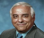
Orlando Auciello
University of Texas Dallas, USA
United States of America
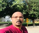
Ratnesh Das
Dr Harisingh Gour Central University, India
India
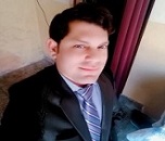
MUJAHID MUSTAQEEM
National Taiwan University (NTU), Taiwan
Taiwan
Abolfazl Ghaderian
Institute of Chemical Research of Catalonia (ICIQ), Spain
Spain
Osman Adiguzel
Firat University, Turkey
Turkey
Media Partners & Collaborations

Media Partner
Media Partner

Media Partner

Media Partner

Media Partner

Media Partner
Media Partner
Media Partner

Media Partner
Media Partner

Media Partner

Media Partner

fgsg
tgh

Dear Eliza, Thank you for that wonderful opportunity given to share my experiences during the conference. I would like to place on record the smooth conduct of the conference. My appreciation goes a long way to Eliza for her timely communication and well advanced information disseminated processes. The presentation schedule and the time mentioned in the mail sent were also strictly followed. All the best. Regards Kalyani Kenneth Speaker | Psychiatry-2021
Kalyani Kenneth

Dear Laura, Thank you for giving me the opportunity to present my current work! I really enjoyed listening and connecting to a wider international scientist through this conference. And I am really looking forward for the physical conference next year! Best regards Sharmaine
Sharmaine Reintar

Many thanks Laura. It iş my plesure work with you
Pinar Kara

It was my pleasure to be a part of the conference. The talks were technically profound. Thank you once again.
Anupam Mukherjee

Thank you very much for the message. I am glad that the presented poster was appreciated. I'm also grateful for the certificate. Dispite my main work was the subject presented in the session, it would be a pleasure to participate in the webinars.
Ana Rita Domingues

Thank you for your appreciation. I love the support received from you and your admirable patience from invitation till the end of the conference. Thank you very much. I hope to participate in future conferences.
Munezza Khan

Am really grateful for you inviting me to this great event... Am thrilled to be part of this great team, I feel honored 😀😃😄🤝🏻
Aysha Haruna

The conference was arranged nicely through a Webex. I found the sessions interactive and informative. I am looking forward to join the next annual meeting of plant genomics in osaka, japan in april 2022.
Ruchika

Highly appreciate your quick response and I am grateful for all your help.
Dr. P T Sunderam

Informative and Innovative sessions
Michael Lacroix

Delightful event with a wonderful sessions
Mohamed Ebraheem Elmesserey

Very much grateful for this opportunity to share the innovative ideas
Mahmoud Metwaly Taha

It was really informative and excellent platform to share the research ideas
Raktima Chakrabarti

Wonderful experience
KHALED NASR ELDIN REYAD

Thank you very much for organizing this wonderful conference
JIMMY KAYASTHA

it was impressive and left me a very good memory.
VAISHALI SAMIR JOSHI

I learnt a lot from the conference and hope to attend the next conference
Deepak Mane

It was a nice and well-organized meeting! Thank you for all your efforts of having put it together.
Vladimir Startsev

The conference was exciting. I enjoyed so much meeting new colleagues at the venue. I would like to express my sincere gratitude to you for your assistance and opportunity. It was a good experience attending this conference.
Daniela Capdepon

It was great being a part of Surgery 2021
Hadi Nural

How much I appreciate your support, you and your job are meaningful. I always wish the best for you. Thank Laura a lot
Kevin Ton

Hats off to you and fellow organizers. Great opportunities for sharing and networking!
Karen Swanepoel

It was a pleasure to participate in this year’s meeting (even in webinar format due to the COVID-19 pandemic) and I hope the participants enjoyed my talk. There were some interesting talks taking place today and the whole experience was enjoyable like last year. Please rest assured that I will be happy to join next year’s meeting as well, hopefully with a physical presence.
Vasileios Fotopoulos

It was my pleasure to attend this conference. Thanks for your kind efforts.
Saeed Taheri

Thank you for your effort for having made "Pharmacology 2019 conference" wonderful success. Thank you again for that.
Ryong Nam Kim

Thanks for holding a nice conference.
Ramin Ataee

I enjoyed the conference. Italy will be a great place to have the next conference. I look forward to 2020 edition.
Paul Njiruh Nthakanio

I am very happy to make a seminar in the conference. If I have a chance to present my work in your conference, I would talk it in your conference in future.
Takayuki Momma

It was good to connect with a diverse group of scientists - thanks very much for the invite
Thomas P Brutnell

It was a nice experience for me to attend plant genomics conference in Osaka and meet researchers from different countries.
Behnam Derakhshani

It has been an excellent experience.Thank you a lot for this opportunity. I enjoyed it very much!
Julio Cesar Vega

I definitely would like to join your conference again. It was so great about everything. I think I would say great coordination and services.
Maryam Jenabi

Great experience being a part of this conference as a moderator
Soizic de Beaucorps

Amazing experience full of knowledge and meeting new people. Looking forward to being back
Thomas Frederick Hartley

Thanks a lot. It was an excellent event. Really enjoyed.
Umesh Prabhu

It was a pleasure and a great opportunity to be one of the Keynote speakers. I welcome the opportunity to speak at additional conferences in the future. Please keep my contact information for future consideration.
Sharon Nixon-Crenshaw

Thank you for assisting in my participation in a superbly organized Conference. I especially appreciate that you made a special session for me. And once again, sincerely thank you for inviting me to the Conference.
Albert Krashenyuk

Thank you for all your help for the meetings. It was for me a great experience to be in a kind and so scientific group.
Katia lollai

I enjoyed a lot thank you. I thank Meetings International for the quality of the event. All the speakers i had notice of were well prepared and highly motivated Compliments!
Dora Dragoni Dıvrak

Thank you for organizing the conference. It was nice to partake in the event.
Marcello Menapace

I enjoyed participating in the congress and thank you for your efforts to make it easy for participants. Please keep me in mind for future meetings.
Debendra Kumar Tripathy

It was a nice meet and we had a wonderful time in Paris Thank you once again for the arrangement. I would be interested in participating future meetings.
Prasanna Udupi Bidkar

Thank you so much for giving me a chance to my research presentation in your conference.
Seyedataollah montazam

I enjoyed being in the conference. Thanks for you excellent arrangement for my participation. Looking forward for next meetings.
Afaf El Ansary

The conference is very nice, Thank you so much for inviting me to your esteemed event.
Esmira Naftali

The conference was very good. I hope to attend similar meeting in future. Thank you .
Lia Monica Junie

I am indeed glad to acknowledge that for last two days during Optics-2018, International conference on Lasers, Optics and Photonics it was Successfully conducted and we had very fruitful discussions and interactions to make many great friends for life. Many Delegates had interactions with many famous Japanese University Professors and company Managers too for their future possibilities of R&D collaborations. I had arranges a session for such interactions while eating and discussing with relaxed environment and taking group pictures. The hospitality provided by your Organization Committee Members was excellent to help completing Conference Inauguration, all Keynote Speeches, Oral Presentations And Poster session had very high-quality research presentations in many advanced research areas such as Spectroscopy, Ultra high power Lasers, Fibers, Advances in stabilized high frequency mode-locked pulsed Fiber Lasers, MEMS, Optical Interconnects, Photonics and Advanced Optical Biomedical Imaging, THz and optical communications and Interconnects, theoretical and experimental research and so on from highly recognized Professors and Researchers in Japan and advanced institutions in many advanced countries.
Dr. Brahm Pal Singh

I wish to thanks you for my perfect time on conferense in Osaka. It was great experience for me.
Anton Podkopaev

I wish to thanks you for my perfect time on conferense in Osaka. It was great experience for me.
Dr. Anton Podkopaev

I would refer this organization future conferences to my colleagues and also love to join again in diabetes related events. More topics on diabetes should be there in future diabetes conferences.
Radia Boufermes

Thank you for the invitation and the opportunity to participate. It was very good.
Juliana Francisca Grossi Heleno

Thank you very much for the invitation and it was a great honor for me to join this conference. I had a great time.
Alkis Konstantinopoulos

It was a good event and got to make good friends out there.
Nur Ozel

Thank you so much. Really we appreciate the Congress, hope next time it will be longer. Everything was ok, the venue, colleagues, organizing team. Thank you and hope to meet soon in other Congress soon.
Sameh Samy Abdou

It was a great pleasure of mine to be there during the conference looking forward to joining your future conferences
Ahmed Halim Ayoub

The theme of the conference and the scientific panel are very interesting! I am looking excited to learn many new things on this innovative platform
Lisa mattheu

I would love to attend the Infectious Diseases 2019 conference. The hospitality, the renowned speakers, and the city are awesome. Looking forward to it!
Dr. Ianane Jireh Ramos canizares

Hello Daniel, Thank you for the invitation to the conference. It was an interesting experience. I am glad that my presentation was liked. Like the effects of my work. Stay in touch. Best Regards !
Aneta Zymon

Thank you to Daniel Raybin with Wound Care 2018 for allowing me to be the Keynote Speaker for the conference. Dr. Jeff Mayo and I met colleagues from other countries such as Poland and Ukraine that work in plastic medicine and surgery. We are excited to share our knowledge of wound care in the veterinary industry so that our human medicine counterparts can offer the same standardized care that we utilize in the US. Thank you to Regenlabs for sponsoring the event and Jorgensen Laboratories for providing us with a great sponsor to represent our mission.
Nicole LaForest

Dear Daniel! Thank you for the conference, for your accommodation and the opportunity to see the most romantic, mysterious, fabulous Amsterdam
Nadiia Nor

Congress was good, the quality of the presentations was good. The choice of Singapore as strategic headquarters has been good
Buonocore D

Thanks for your invitation. I enjoyed participating at he conference in Rome and am interested in participating again next year in Paris.
Daniel Benetti

Great experience!! Thanks a lot for the opportunity to speak.
Jose Carlos Ferreyra Lopez

Dear Julie, Many thanks to you as you offered me this opportunity to come and participate at this valuable event in Chicago. I think you are great professional and made huge efforts for the event in terms of organization, engaging speakers, etc. And also you have sense for people, act as empathic person what is very important for me. I was very happy and honored to be invited as a speaker at World Biosimilars Conference in terms to present company Ewopharma AG as business partner of different pharma companies in Central and Eastern Europe, especially company Biogen with its portfolio of biosimilars and share my commercial experience in launching biosimilars! I found the conference interested in terms you selected very qualitative speakers from different areas: innovation and science, manufacturing and commercialization. From my perspective, the most interesting topics were: Sarfaraz K Niazi: “Biosimilars: Why are they so widely misunderstood?” Ronald P Dudek: “The adapter CAR Platform: From antibody to CAR T cell therapeutic” Jose Carlos Ferreyra Lopez: “Market access barriers and market value in Mexican public sector for biosimilars” Milind Antani: “Similar biologics in India- Impact of regulations on business” Joel I Osorio: “RegenerAge System “ (So I will be very happy if you could share these mentioned presentations with me!). I can see more potential for further improvement to put 100% focus on Biosimilar topics and to attract more specialists/professionals to gather. It will be excellent if you could attract more speakers from Europe to share their experience. So please consider this option how to attract them in the future (if I got some nice ideas will share with you!).
Sandra Simic

Thanks for giving opportunity to share my research at 3d printing conference .I meet global experts and exchange our ideas.Two days conference are going very good ,workshop session,exhibition .I felt moved to contribute next year also..
Rajkumar Velu

It is wonderful conference of 3d printing & Bio printing in health care .participates are coming from world wide 3d printing & Bio printing experts .Workshop sessions is too good .
Lifeng Kang

• Good workshop session at conference with lots of discussion among audiences and speakers about the regulatory aspect of 3D printed medical devices. • Many of the topics were good and interesting. • It will be good if the organizer could have invited more participants as well as selecting the speakers based on proven and relevant track record. • It will be better if there are people who keep track of the time for each topic.
Albert Sutiono

Conference was superb. It was well conducted. I appreciate all the speakers, presenters and organizers. I am very proud to be part of this event.
Rajani singh

We had a very good session at cardiomersion in which we discuss about the integrated cardiomersion approach to the delivery of cardiovascular case. Thank you to all the speakers who came across the globe. Finally I would like to thank the organizers for making such a remarkable event.
Deepak Puri

I have been a part of this conference and I am very proud to see the conference very well organized and people are helping us and each other to present their case reports and research. Thank you very much to the organizers for making such great events
Suresh Vatsyayan

The event was very nice and I want to thank all the participants, presenters and the organizers. We hope in future we will have more events like this
Yuan Chen

The BABE conference was very interesting and lot of scientific sessions were covered and highlighted. Special thanks to the Organizing Members and the participants
Kateryna Zupanets

Conference was good, thanks for organising. I felt moved to contribute throughout, and felt that to a certain extent I acted as a moderator throughout the event .It is very happy for me.
Alexander M. Korsunsky

I want to express my graduate and thanks to you for all efforts you put to organize such a successful conference. For 2 days I enjoyed the company of brilliant and beautiful minds from all over the world. I had a great chance to exchange expercties with them and in large my horizons. I want to thank you again for organizing the International Conference of Petroleum Engineering 2018, Dubai, UAE and hope to meet you again very soon.
Essa Georges Lwisa

I enjoyed participating in the congress and thank you for your efforts to make it easy for participants. Please keep me in mind for future meetings relating to bariatric surgery, I would be interested in participating or being part of the organizing committee.
Peter Harris

Meetings International meetings are great way to receive way to receive other scientists in different parts of the world doing, These meetings provides the opportunity for you to work at latest concepts from different peoples also specifically it allows the opportunity to call to the new relationships when it resolves in future collaboration across the photolamps
Suzanne Tinsley

I enjoyed conference with Meetings International it is a mutal legitimate.It is always with first move which encourages scientists for practicing ability based practice It also gives lots of opportunity for discussions as well as collaborations in future
Dr. Marie Vazquez Morgan

We enjoyed the meeting so much. Wish you all success in the coming meetings.
Richa Jaiswal

It was a great experience for us to attend the conference. Had good interactions with speakers. Many thanks to you and Mr Peter Harris for giving us opportunity to participate and visit Japan as well. Wish to attend further conferences in future!
Kalpana Kulkarni

The first day was very good. It was meaningful to spend academic meeting. I thank you for your consideration.
Gagan Dhall

International meeting was good looking forward for next meetings.There can be more we can do because there is always scope for improve.
Suman Lata

Thanks for your greeting letter! We enjoyed the conference. Sure! We will meet again in 2019!
Dra Milagrosa C. S. Liu

First of all I would like to say many thanks to YOU and The Organization / Planning Committee, for I have been given the opportunity to join in this very Prestigious Event. I am also grateful to meet with researchers from other countries who have innovative research’s. Hopefully it could upgrade to my knowledge and more increases my interest in this field of science. Nice to join in this event I wish i could be join on the Traditional Medicine 2019.
Yunita Sari Pane

It was great experience for me. My talk was very much liked by all receipients at Osaka.
Mohammad Kamil

I am indeed glad to acknowledge that for last two days during Optics-2018, International conference on Lasers, Optics and Photonics it was Successfully conducted and we had very fruitful discussions and interactions to make many great friends for life. Many Delegates had interactions with many famous Japanese University Professors and company Managers too for their future possibilities of R&D collaborations. I had arranges a session for such interactions while eating and discussing with relaxed environment and taking group pictures. The hospitality provided by your Organization Committee Members was excellent to help completing Conference Inauguration, all Keynote Speeches, Oral Presentations And Poster session had very high-quality research presentations in many advanced research areas such as Spectroscopy, Ultra high power Lasers, Fibers, Advances in stabilized high frequency mode-locked pulsed Fiber Lasers, MEMS, Optical Interconnects, Photonics and Advanced Optical Biomedical Imaging, THz and optical communications and Interconnects, theoretical and experimental research and so on from highly recognized Professors and Researchers in Japan and advanced institutions in many advanced countries.
Dr. Brahm Pal Singh

I wish to thanks you for my perfect time on conferense in Osaka. It was great experience for me.
Dr. Anton Podkopaev

Interesting presentation & worthfull spirit of exchange of experience
Ippei Sakamaki

Thanks a lot we hade a great time and grest conference. We enjoyed the conference .
Chi-Ying Huang

I would like to express my gratitude for your engagement in preparation of the Cancer Therapy Summit 2018. It was a valuable experience.
Hong Qin

Conference was good. Thanks for your support and co operation.
GURUSAMY MARIAPPA

My active partecipation to the Toronto meeting is just over and motivated by it and by Joseph Ndisang who I met there, I'd like to ask and verify whether I could further collaborate more actively, with no expenses for it, within yr network with my long term scientific expertise and long background in the field of diabetes and also at the light of my previous experience with you over the last year.
Marco Songini

“ The organisation and coordination of the international conference of nanotechnology and nanoengineering was at an outstanding level, it was a great honour to participate in such phenomenal event “
Ahmed Abushomi

I also really appreciated all the scientific contact I made within all these participants - Think that in the future if you might request some help for that renewal activity, I might be helping your team of course (I have some suggestions for making better sort / type of presentation activities for invited speakers of course according to my experience in the field).
Jean-paul Lellouche

The conference sesions proceeded successfuly in a hot and friendly atmospher. I observed during the conference every delegate and speaker interacted wit each other and made friend. I am sure that the conference has become a scientific platform to exchange knowledge among the scientists from all over the world, and they wil conduct a new collaborations. During the conference, onsite organizers spent a great efford. I believe that the level and quality and reputation will increase year to year. Unexpected and unavoidable circumstances can occur at everywhere and every activation, and they can be solved easily. Hope to meet you and your team in another conference.
Osman Adiguzel

Thank you for your friendly mail. I enjoyed the conference with interesting speakers. I did not know anybody at the beginning but I found good companions during the conference.The hotel was good but it was located somewhat outside of Paris. Nevertheless, we had a good time. Anyway, thank you again for your invitation.
Nikolaus Stolterfoht

Thank you. Yes the conference was really interesting.
Adil Aghzar

Thank you! I also think that the event was very successful and very interesting. The variety of thematic session and possibility to meet experts from different fields of marine biology and aquaculture was the biggest advantage of the conference. However, it might be useful to attract more participants to next conference.
Magdalena Jakubowska

Thank you for your kind welcome and appreciated support during the appreciable meeting. Thank you for your kind offer to continue to cooperate to this interesting initiative and I am available to cooperate again in remote and to eventually attend the conference. Thank you and your colleagues and the scientific valuable people that attended the conference for your kind cooperation.
Gianluca Ragusa

Thank you for allowing me to participate in this event, I liked the organization and the people who participated, I made many friends too. Of course I would like to collaborate with you in organizing the next Aqua 2019 conference.
Alfredo Olivera Galvez

The meeting was a success with many experience professional.
Nyan Taw

A very thorough and well written set of points. It’s great that you took the time to put this together.
Feng Gao

Thank you for offering an unforgettable experience for all of us. We are honored to attend the conference. We are so happy and thanks a lot.
Stef Stienstra

Many thanks for your continuous support throughout the conference. It was the pleasure to participate and shared the findings at such high level meetings.
Pooja Jain

The conference was very enjoyable and I was honoured to be able to present my research at this prestigious event. The conference was particularly good for me as it is always important to keep up with the new developments
Glenda Gray

I had a wonderful time at the conference and learned so much from the presenters. Thank you kindly for putting this event together.
Marc HV Van Regenmortel

I had a great time in the conference, Everythings are OK, thank you .
Hsiao-Hui Chiu

Wonderful!! thank you for all the help you have done
Sharadha Ramesh

Thank you for your arrangement. Our team enjoyed the meeting so much. Wish you all success in the coming meetings!
CHAN Yui Fung

Surely we will maintain our relation in long run. If there is any opportunity for me to start my carrier being fresher and any guidance from you to me. It will be highly appreciated.
Monika kankarwal

I appreciate your polite contact. I enjoyed my first visit to Singapore. It was meaningful to spend academic meeting. I thank you for your consideration.
Kazue Sawami

Thank you for the email ,it was my sincere honor and pleasure to participate , many thanks for the invitation ,well organised conference, great hospitality ,well composed programme,interesting nursing topics, but not very large group size enough group size to be conducive to excellent discussions, I wish you all the success for your further conference
Hana Kadhom

Thank you for successful conference in Singapore. And thank you for giving me opportunity of oral presentation. It was very good experiences to me.
Hyun, Myung sun.